Wednesday, July 31, 2013

0 Comments
Posted in Arrangement, Art, Business

USB Power Booster

The USB serial bus can be configured for connecting several peripheral devices to a single PC. It is more complex than RS232, but faster and simpler for PC expansion.Since a PC can supply only a limited power to the external devices connected through its USB port, when too many devices are connected simultaneously, there is a possibility of power shortage. Therefore an external power source has to be added to power the external devices.
Circuit diagram:
USB Power Booster Circuit-Diagram
USB Power Booster Circuit Diagram
In USB, two different types of connectors are used: type A and type  B. The circuit presented here is an add-on unit, designed to add more power to a USB supply line (type-A). When power signal from the PC (+5V) is received through socket A, LED1 glows, opto-diac IC1 conducts and TRIAC1 is triggered, resulting in availability of mains supply from the primary of transformer X1. Now transformer X1 delivers 12V at its secondary, which is rectified by a bridge rectifier comprising diodes D1 through D4 and filtered by capacitor C2.
 Pin configurations of moc302Pin configurations of moc3021, bt136 and 5v regulator 7805
Regulator 7805 is used to stabilise the rectified DC. Capacitor C3 at the output of the regulator bypasses the ripples present in the rectified DC output. LED1 indicates the status of the USB power booster circuit. Assemble the circuit on a general-purpose PCB and enclose in a suitable cabinet. Bring out the +5V, ground and data points in the type-A socket. Connect the data cables as assigned in the circuit and the USB power booster is ready to function.


http://www.ecircuitslab.com/2011/12/usb-power-booster.html

Tuesday, July 30, 2013

0 Comments
Posted in Arrangement, Art, Business

5 to 15V Regulated Power Supply Rise

Regulated Power Supply
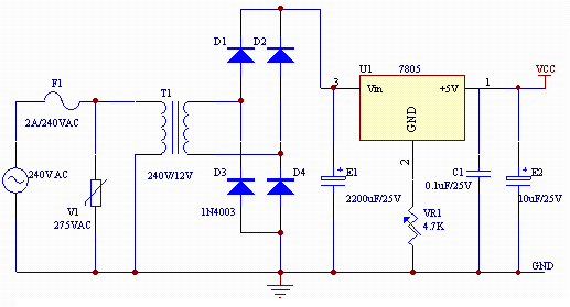
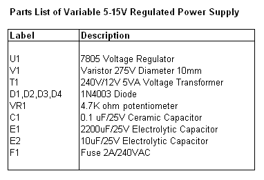
This project is a normal DC regulated power supply that is a variable DC voltage range from 5V to 15V. It can supply current up to  400mA to power the various circuits for your electronic projects. The voltage output is varied by using the potentiometer V.R1. In this circuit, the input line power supply is designed for 240V.A.C. If 110VAC input is used, alter the ratings of the varistor to 150VAC & the transformer ratio to 110V/12V. 

Fuse F1 is used as a protection in case theres any short circuit in the circuit. Varistor V1 is connected in parallel to the input of the line voltage to clamp the surge voltage from the line to a reasonable level that helps to protect the transformer & other circuitry. One time the voltage level surge to a high level beyond the ability of the varistor to absorb it, fuse F1 or varistor V1 or both will burn. If this circuit failed after a period of operation, check that the fuse & the varistor are still in nice condition or else replace them.

Diodes D1, D2, D3 and D4 are used to rectify the 12V.A.C voltage to DC voltage. Electrolytic capacitor E1 is used as a smoothing capacitor to reduce the ripple of the DC voltage. The DC voltage is fed in to the input of 7805 regulator where the output DC voltage is obtained. Changing the worth of VR1 will alter the output of the DC voltage. Capacitor C1 is used to filter out high frequency part from the power supply.


0 Comments
Posted in Arrangement, Art, Business

Simple Stereo VU Meter

I like to see lights move to music. This project will indicate the volume level of the audio going to your speakers by lighting up LEDS. The LEDS can be any color so mix them up and really make it look good. The input of the circuit is connected to the speaker output of your audio amplifier. You want to build two identical units to indicate both right and left channels. The input signal level is adjusted by the 10k ohm VR. If you wish to make a very large scale model of this unit and hang it on your wall there is an optional output transistor that can drive many LEDS at once. The unit I built drove three LEDS for each output. The sequence of the LEDS lighting are as follows Pin 1, 18, 17, 16, 15, 14, 13, 12, 11, 10.


Streampowers

Monday, July 29, 2013

0 Comments
Posted in Arrangement, Art, Business

Laser Level Detector

Rotating laser levels, which are very handy  for setting objects in a room or garden at the  same height, are available at prices of a few  dozen pounds. At relatively large distances  and for outdoor use, the light from the rotating laser beam is often not easy to see, and  the laser beam detector described here can  be useful in such situations. The detector  works well at distances up to 50 metres (150  feet) and consists entirely of standard components. The detector is housed in a plastic case  that can be fixed to an object (such as a post  or a beam). It has three LEDs and a beeper that  indicate whether the object should be raised  or lowered.
Laser Circuit 1
LEDs with a transparent package and integrated lens (round surface) are used as sensors. The top and bottom detection zones  each have five LEDs and two opamps (IC1a &  IC1b or IC1c & IC1d), which drive the ‘Move  Up’ and ‘Move Down’ indicator LEDs. The middle sensor LED drives the ‘OK’ indicator LED  via two opamps (IC2a & IC2b).  The rising edges of the opamp output signals  trigger three separate monostable multivibrators (type CD4047). If desired, the circuit  shown inside the dashed outline (one gate of a  CD4044 quad RS latch) can be used in place of  each of the monostable multivibrators. In this  case the output signal has the opposite polar-ity, so the BS170 N-channel MOSFET must be  replaced by a P-channel type.
Laser Circuit 2

The monostable time of the middle retriggerable MMV should be longer than the rotation period of the laser (e.g. with a 2 rpm laser  it should be longer than 500 ms) so that the  beeper will emit a continuous tone. Most  rotating laser levels have variable speed, so  this can also be achieved by adjusting the peed if necessary. The monostable times of  the upper and lower MMVs are dimensioned  to generate clearly distinguishable short and  long beeps, respectively. The three MOSFETs  (T1, T2 and T3) are configured as a wired-OR  gate to drive the shared beeper. The fourth  MOSFET (T4) drives the ‘OK’ LED.
The circuit can be housed in an enclosure  together with three penlight cells.

Source: http://www.ecircuitslab.com/2012/05/laser-level-detector.html


Thursday, July 25, 2013

0 Comments
Posted in Arrangement, Art, Business

2 5A 1 25 To 25V Regulated Power Supply Circuit Diagram

This power supply uses an LM317J adjustable regulator and an MJ2955 pass transistor. Ql and U2 as well as Ul should be heats inked. A suitable heat-sink would typically be 4` 4` 1` fins, extruded type, because up to 65 W dissipation can occur. R8 and R9 should be 1% types or selected from 5% film types with an accurate ohmmeter. Capacitors are disc ceramic except for those with polarity marked, which are electrolytic. D1, D2—1-A, 100-PIV rectifier diode. DS1—Red LED. F1 —1,5-A, 3AG fuse in chassis-mount holder. J1, J2—Standard five-way binding post, one red, one black. M1—Milli-ammeter, 0-1 mA dc. Q1—NPN power transistor MJ2955 (Radio Shack) or equiv device with a + 70-V, 10-A, 150-W rating in a -204 case. R1, R2, R7—5-W wire-wound resistor. See Notes 3 and 4 for source, or, use 17 inches of no. 28 enam wire, single-layer wound, on a 10-KOhmhm, 1-W carbon-composition resistor for R1 and R7. For R2, use 36 inches of no. 30 enam wire on a 10-KOhmhm, 1-W carbon composition resistor (scramble wound). R-4—Panel-mount, 5-kfi, 2-W or 5-W potentiometer, carbon or wire wound (See Note 8). R8, R9—See text. 51—SPST toggle switch. 52—DPDT toggle or rotary wafer switch. T1—25.2-V, 2.75-A power transformer (see text). U1—6-A, 200 PIV bridge rectifier with heat sink. See text. U2—LM317T +1.25- to 30-V, 1.5-A 7-220 regulator. Use an LM317HVK (T0-204 case) for dc output voltage greater than 40. See text.

2.5A-1.25 To 25V Regulated Power Supply Circuit Diagram

2.5A-1.25 To 25V Regulated Power Supply Circuit Diagram

Saturday, July 13, 2013

0 Comments
Posted in Arrangement, Art, Business

2 4GHz WiFi ISM Band Scanner Assembly Using the Scanner Part 3

2.4GHz WiFi & ISM Band Scanner. Description and Schematic - Part 1

2.4GHz WiFi & ISM Band Scanner. Firmware and Sowtware - Part 2

 
Assembly

Because the circuit was so simple I took the easy way out and assembled it on a piece of veroboard. Nowadays I would design my own printed circuit board (see custom PCBs).

Rather than finding a connector for the Cypress module I simply soldered single core hookup wire directly to the connector pins. This supported the module and allowed me to position it away from the microcontroller to minimise interference.

The USB cable was made from a standard USB cable with type A and B connectors, I just cut off the B connector and soldered the wires directly to the veroboard with half an inch of heatshrink tubing to keep it neat. That left the type A connector at the other end, ready to plug into the computer.

Note that the red and black wires in the USB cable are +5V and ground respectively. You should check these with a multimeter before soldering them in. The green wire is normally D+ and goes to pin 16 of the 18F2550 while the white is D- and goes to pin 15. The shield does not have to be connected.

The final touch was to drop the assembly into a standard UB5 "jiffy" box with a notch cut out for the USB cable to pass through.

2.4GHz WiFi & ISM Band Scanner

Using the Scanner

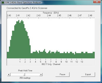
With nothing running in the immediate vicinity you will just see background noise, as shown in the screen shot below.

2.4GHz WiFi & ISM Band Scanner

Note that the vertical scale is not calibrated to any particular scale. In fact the scale is just the signal level "factor" reported by the Cypress radio module.

The base level signal represents the noise in the air and in the radio receiver part of the module.

The screenshot below shows a WiFi 802.11n wireless router running on channel 1 and located about 12 metres from the scanner. As you can see the 802.11n (and for that matter 802.11g) routers spread themselves over six channels.

2.4GHz WiFi & ISM Band Scanner

That is the good thing about using channel 1 and 13 for your WiFi setup, you get some unused channels on one side where your spectrum can spread into.

But, using channel 13 has its own problems.

The spectrum on the next screenshot is identical to the one above but this time my microwave oven was heating up dinner. Incidentally, the microwave oven was nothing special, just a domestic model and about 10 metres from the scanner.

2.4GHz WiFi & ISM Band Scanner

As you can see, it totally blotted out the higher frequency end of the band. All microwave ovens seem to use this part of the band and you cannot blame the microwave for their activity, as this was part of the reason for setting up the 2.4GHz ISM band in the first place. Avoiding the microwave oven interference and having some free spectrum on one side is the reason why channel 1 is the best choice for your router (assuming your neighbour has not got there first).

Finally, the screenshot shows a Bluetooth mouse communicating with a computer.

2.4GHz WiFi & ISM Band Scanner

Bluetooth hops all over the 2.4GHz band as it finds the best spots with the minimum of interference. Spikes all over the spectrum is a good indicator of Bluetooth activity. 

Friday, July 12, 2013

0 Comments
Posted in Arrangement, Art, Business

Simple Over Current Indicator

Simple Over Current Indicator
This circuit eventually surfaced while pondering over the design of a current indicator for a small power supply. Fortunately, it proved possible to employ the supply voltage as a reference by dividing it down with the aid of R1 and R2. C1 is an essential capacitor to suppress noise and surges. The half supply voltage level is applied to the non-inverting pin of opamp IC1. The value of the R3 determines the trip level of the indicator, according to

R3 = 0.4 × (desired voltage drop) / I trip

Actually this is high side sensing but the method can be used as low side sensing, too! The desired voltage or sense voltage can be any value between 0.35 V and 0.47 V. If currents greater than about 1A are envisaged, you should not forget to calculate R3’s dissipation on penalty of smoke & smells.

Another voltage divider network, R4, R5 and P1 divide the voltage between supply voltage and desired oltage. This divided voltage, filtered by C2, is fed to the inverting input of IC1 to compare levels. The result causes D1 to light or remain off. Turn P1 to the end of R4 to hold off D1. Then connect a load causing over current and adjust P1 towards the end of R5 until D1 lights. The accuracy of the circuit depends entirely on the tolerances of the resistors used - high stability types are recommended.

Thursday, July 11, 2013

0 Comments
Posted in Arrangement, Art, Business

USB Power Booster

The USB serial bus can be configured for connecting several peripheral devices to a single PC. It is more complex than RS232, but faster and simpler for PC expansion.Since a PC can supply only a limited power to the external devices connected through its USB port, when too many devices are connected simultaneously, there is a possibility of power shortage. Therefore an external power source has to be added to power the external devices.
Circuit diagram:
USB Power Booster Circuit-Diagram
USB Power Booster Circuit Diagram
In USB, two different types of connectors are used: type A and type  B. The circuit presented here is an add-on unit, designed to add more power to a USB supply line (type-A). When power signal from the PC (+5V) is received through socket A, LED1 glows, opto-diac IC1 conducts and TRIAC1 is triggered, resulting in availability of mains supply from the primary of transformer X1. Now transformer X1 delivers 12V at its secondary, which is rectified by a bridge rectifier comprising diodes D1 through D4 and filtered by capacitor C2.
 Pin configurations of moc302Pin configurations of moc3021, bt136 and 5v regulator 7805
Regulator 7805 is used to stabilise the rectified DC. Capacitor C3 at the output of the regulator bypasses the ripples present in the rectified DC output. LED1 indicates the status of the USB power booster circuit. Assemble the circuit on a general-purpose PCB and enclose in a suitable cabinet. Bring out the +5V, ground and data points in the type-A socket. Connect the data cables as assigned in the circuit and the USB power booster is ready to function.


http://www.ecircuitslab.com/2011/12/usb-power-booster.html

Wednesday, July 10, 2013

0 Comments
Posted in Arrangement, Art, Business

Simple Li Ion Battery Charger

The LP2951 regulator is manufactured by National Semiconductors. The choice of values is from an application note Battery Charging, written by Chester Simpson. Diode D1 can be any diode from the 1N00x series, whichever is conveniently available. It functions as a blocking diode, to prevent a back flow of current from the battery into the LP2951 when the input voltage is disconnected. Charging current is about 100+mA, which is the internally-limited maximum current of the LP2951. For those wondering, this is compatible with just about any single-cell li-ion battery since li-ion can generally accept a charging current of up to about 1c (i.e. charging current in mA equivalent to their capacity in mAh, so a 1100mAh li-ion cell can be charged at up to 1100mA and so on).

Li-Ion Battery Charger Circuit Diagram A lower charging current just brings about a correspondingly longer charge time. IMHO 100mA is quite low, low enough that the circuit can be used for an overnight charger for many typical single-cell li-ion batteries. The resistors are deliberately kept at large orders of magnitude (tens/hundred Kohm and Mohm range) to keep the off-state current as low as possible, at about 2?A. Resistor tolerances should be kept at 1% for output voltage accuracy. The 50k pot allows for an output voltage range between 4.08V to 4.26V - thus allowing calibration as well as a choice between a charging voltage of 4.1V or 4.2V depending on the cell to be charged. The capacitors are for stability, especially C2 which prevents the output from ringing/oscillating.

Parts List

IC1 = LP2951, voltage regulator
D1 = 1N4002, General purpose diode
R1 = 2M, 1%, metal-film
R2 = 806K, 1%, metal-film
P1 = 50K, potentiometer
C1 = 0.1uF, polyester
C2 = 2.2uF/16V, electrolytic
C3 = 330pF, ceramic

Tuesday, July 9, 2013

0 Comments
Posted in Arrangement, Art, Business

A Low Cost Hearing Aid Circuit

Small and portable unit, Useful for old men and old women

This low-cost, general-purpose electronic hearing aid works off 3V DC (2x1.5V battery). The circuit can be easily assembled on a veroboard. For easy assembling and maintenance, use an 8-pin DIP IC socket for TDA2822M.

Circuit Diagrams:
Hearing Aid Circuit A Low Cost hearing Aid Circuit
Parts:
P1 = 10K
R1 = 2.2K
R2 = 330K
R3 = 680R
R4 = 33R
R5 = 100R
R6 = 4.7R
R7 = 4.7R
R8 = 220R
C1 = 0.01uF-10V
C2 = 100nF-63V
C3 = 47uF-10V
C4 = 10uF-10V
C5 = 0.01uF-10V
C6 = 100uF-10V
C7 = 100nF-63V
C8 = 100nF-63V
D1 = Red LED
Q1 = BC547
IC1 = TDA2822M
EP1 = Mono Earphone 32R
SW1 = On-Off Switch

Circuit Operation:

In this circuit, transistor Q1 and associated components form the audio signal preamplifier for the acoustic signals picked up by the condenser microphone and converted into corresponding electrical signals. Resistor R5 and capacitor C3 decouple the power supply of the preamplifier stage. Resistor R1 biases the internal circuit of the low-voltage condenser microphone for proper working. The audio output from the preamplifier stage is fed to the input of the medium-power amplifier circuit via capacitor C2 and volume control P1.

The medium-power amplifier section is wired around popular audio amplifier IC TDA2822M (not TDA2822). This IC, specially designed for portable low-power applications, is readily available in 8-pin mini DIP package. Here the IC is wired in bridge configuration to drive the 32-ohm general-purpose monophonic earphone. Red LED (D1) indicates the power status. Resistor R8 limits the operating current of D1. The audio output of this circuit is 10 to 15mW and the quiescent current drain is below 1 mA.
Source by : Streampowers
0 Comments
Posted in Arrangement, Art, Business

Simple RF Amplifier

This RF amplifier circuit diagram is a very simple and is designed to work for 10 meters band (26 ... 30 MHz) reserved for amateurs. By making this RF amplifier small power transmitters of 200 mW, can be transformed into a power transmitters reasonable, ranging between 2 and 3 W. The circuit is very simple. Network output filter suppresses noise by at least 55 dB.

Simple RF Amplifier Circuit diagram

Amplifier is suitable for almost all types of transmissions, because of the possibility of adjusting the drain current of FETs by P1. For linear applications (AM and BLU), drain current must be adjusted to 20 mA. If is used for FM-CW, P1 will be adjusted so that no current will not flow through the drain rest. For this case, the idle current is 200 mA and between 300 mA.

Coils are made on cases with a diameter of 9 mm. Care should be taken to wound as tight turns without any space between them. Coils should be made as follows: L1 = 12 turns enamelled 0.6 mm copper, L2 and L4 = 5 turns 1 mm enamelled copper, L3 = 8 1 mm enamelled copper coils.

Monday, July 8, 2013

0 Comments
Posted in Arrangement, Art, Business

Motorbike Alarm

This simple to build alarm can be fitted in bikes to protect them from being stolen. The tiny circuit can be hidden anywhere, without any complicated wiring. Virtually, it suits all bikes as long as they have a battery. It doesnt drain out the battery though as the standby current is zero. The hidden switch S1 can be a small push-to-on switch, or a reed switch with magnet, or any other similar simple arrangement. The circuit is designed around a couple of low-voltage MOSFETs configured as monostable timers. Motorbike key S2 is an ignition switch, while switch S3 is a tilt switch. Motorbike key S2 provides power supply to the gate of MOSFET T2, when turned on. 
 
When you turn ignition off using key S2, you have approximately 15 seconds to get off the bike; this function is performed by resistor R6 to discharge capacitor C3. Thereafter, if anyone attempts to get on the bike or move it, the alarm sounds for approximately15 seconds and also disconnects the ignition circuit. During parking, hidden switch S1 is normally open and does not allow triggering of mosfet T1. But when someone starts the motorbike through ignition switch S2, MOSFET T2 triggers through diode D1 and resistor R5. Relay RL1 (12V, 2C/O) energises to activate the alarm (built around IC1) as well as to disconnect the ignition coil from the circuit. Disconnection of the ignition coil prevents generation of spark from the spark plug. Usually, there is a wire running from the alternator to the ignition coil, which has to be routed through one of the N/C1 contacts of relay RL1 as shown in Fig.1 Fig.2 shows the pin configurations of SCR BT169, MOSFET BS170 and transistor BC548.
 
Circuit diagram :

Motorbike Alarm-Circuit-Diagram
 Motorbike Alarm Circuit Diagram
Motorbike Alarm-Pin Configurations :

Motorbike Alarm-Pin configurations
Pin configurations of BT169, BS170 and BC548
 
Also, on disconnection of the coil, sound generator IC UM3561 (IC1) gets power supply through N/O2 contact of relay RL1. This drives the darlington pair built around T3 and T4 to produce the siren sound through loudspeaker LS1.  To start the vehicle, both hidden switch S1 and ignition key S2 should be switched on. Otherwise, the alarm will start sounding. Switching on S1 triggers SCR1, which, in turn, triggers MOSFET T1. MOSFET T1 is configured to disable MOSFET T2 from functioning. As a result, MOSFET T2 does not trigger and relay RL1 remains de-energised, alarm deactivated and ignition coil connected to the circuit.  Connection to the ignition coil helps in generation of spark from the spark plug. Keeping hidden switch S1 accessible only to the owner prevents the bike from pillaging. Tilt switch S3 prevents attempt to move the vehicle without starting it. Glass-and metal-bodied versions of the switch offer bounce-free switching and quick break action even when tilted slowly. 
 
Unless otherwise stated, the angle by which the switch must be tilted to ensure the contact operation (operating angle), must be approximately 1.5 to 2 times the stated differential angle. The differential angle is the measure of the just closed position to the just open position. The tilt switch has characteristics like contacts make and break with vibration, return to the open state at rest, non-position sensitivity, inert gas and hermetic sealing for protection of contacts and tin-plated steel housing. If you find difficulty in getting the tilt switch, you may replace it with a reed switch (N/O) and a piece of magnet. The magnet and the reed switch should be mounted such that the contacts of the switch close when the bike stand is lifted up from rest.
 
 
Streamcircuits

Sunday, July 7, 2013

0 Comments
Posted in Arrangement, Art, Business

NJU7365 Single Phase DC Brushless Motor

A very simple single phase dc brushless motor driver electronic circuit project can be designed using NJU7365 DC brushless motor driver ic manufactured by New Japan radio Co. LTD .

Circuit Diagram

The NJU7365 is a single phase motor driver ic that include in package MOS FET motor driver , direct PWM input , FG output and thermal shut down circuit . The driver is capable of 1000mA maximum output current and continuous current of 350 mA . This motor driver require few external electronic parts and can be powered from dc power supply from 2 to 5.5 volts .

Saturday, July 6, 2013

0 Comments
Posted in Arrangement, Art, Business

Laptops Cord Stays off Your Lap with this Clip

Someone just got this trick works on all the uni body Mac Books and helps keep your wires and cord under control.

Hacks and Mods: Laptops Cord Stays off your Lap with this Clip

This clip is especially bendy if you are lounging on the sofa with the power-cord-side in towards the cushions. It keeps your MacBooks power cord under control with this trick and to stop it from tugging in you. Its built-in cable clip the one that keeps your cord wrapped around the power brick and clip it to the side of your laptops screen.
Hacks and Mods:   Laptops Cord Stays off your Lap with this Clip
The cable pulls it up off your lap and keeps it neat and tidy not to mention free of crazy fall across the keyboard loops.


Source by : Streampowers

Friday, July 5, 2013

0 Comments
Posted in Arrangement, Art, Business

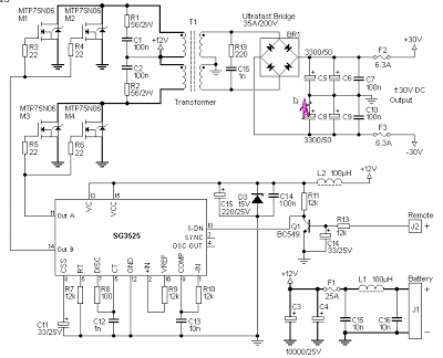
12V to 30V DC to DC Converter Schematic

 12V to +/- 30V DC to DC Converter Circuit Diagram

Converter Circuit Diagram

This is a DC to DC converter for car power amplifier. 12V input generates +30V and -30V output for preamp or power amplifiers. Circuit uses SG3525 IC, Mosfets and switching power supply. 


Thursday, July 4, 2013

0 Comments
Posted in Arrangement, Art, Business

Beat Balance Metal Detector

A Beat Balance Metal Detector made from discrete components.

Beat Balance Metal Detector Schematic


Notes:

Various embodiments of the BB metal detector have been published, and it has been widely described in the press as a new genre. Instead of using a search and a reference oscillator as with BFO, or Tx and Rx coils as with IB, it uses two transmitters or search oscillators with IB-style coil overlap. The frequencies of the two oscillators are then mixed in similar fashion to BFO, to produce an audible heterodyne. On the surface of it, this design would seem to represent little more than a twinned BFO metal detector. However, what makes it different above all else, and significantly increases its range, is that each coil modifies the frequency of the adjacent oscillator through mutual coupling. This introduces the "balance" that is present in an IB metal detector, and boosts sensitivity well beyond that of BFO. Since the concept borrows from both BFO and IB, I have given a nod to each of these by naming it a Beat Balance Metal Detector, or BB for short. Happy hunting!

Wednesday, July 3, 2013

0 Comments
Posted in Arrangement, Art, Business

Audio Pre Amplifier

Simple Audio Pre-Amplifier

This simple circuit provides good gain to too audio singnals .
Use it in main of an RF oscillators to make an RF transmitter that is very sensitive to sound

0 Comments
Posted in Arrangement, Art, Business

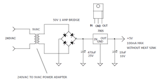
Simple 240VAC TO 5VDC POWER SUPPLY

This is simple way to power some 5v logic from a 240vac source. If a 120vac power adapter is used, the circuit will also work for 120vac power lines.
 
 
240VAC TO 5VDC POWER SUPPLY,

    Total Pageviews